- 您现在的位置:买卖IC网 > Sheet目录2001 > ISL1208IU8-TK (Intersil)IC RTC/CALENDAR I2C 8-MSOP
3
FN8085.8
September 12, 2008
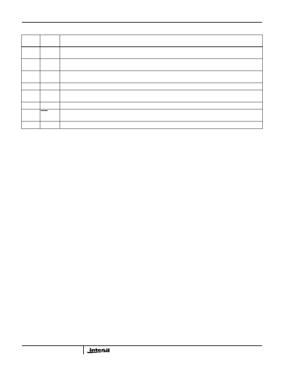
Pin Descriptions
PIN
NUMBER SYMBOL
DESCRIPTION
1
X1
The X1 pin is the input of an inverting amplifier and is intended to be connected to one pin of an external 32.768kHz quartz
crystal. X1 can also be driven directly from a 32.768kHz source.
2
X2
The X2 pin is the output of an inverting amplifier and is intended to be connected to one pin of an external 32.768kHz quartz
crystal.
3
VBAT
This input provides a backup supply voltage to the device. VBAT supplies power to the device in the event that the VDD supply
fails. This pin should be tied to ground if not used.
4
GND
Ground
5
SDA
Serial Data (SDA) is a bidirectional pin used to transfer serial data into and out of the device. It has an open drain output and
may be wire OR’ed with other open drain or open collector outputs.
6
SCL
The Serial Clock (SCL) input is used to clock all serial data into and out of the device.
7IRQ/FOUT Interrupt Output/Frequency Output is a multi-functional pin that can be used as interrupt or frequency output pin. The function
is set via the configuration register.
8
VDD
Power supply
ISL1208
发布紧急采购,3分钟左右您将得到回复。
相关PDF资料
ISL1209IU10-TK
IC RTC/CALENDAR I2C 10-MSOP
ISL1218IUZ
IC RTC LP BATT BACKED SRAM 8MSOP
ISL1219IUZ-T
IC RTC LP BATT BACK SRAM 10MSOP
ISL1220IUZ
IC RTC LP BATT BACK SRAM 10MSOP
ISL1221IUZ
IC RTC LP BATT BACK SRAM 10MSOP
ISL26134AVZ
IC ADC 24BIT SRL 80SPS 28TSSOP
ISL26319FVZ-T7A
IC ADC 12BIT SRL/SPI 16TSSOP
ISL26329FVZ
IC ADC 12BIT SPI/SRL 16-TSSOP
相关代理商/技术参数
ISL1208IU8Z
功能描述:实时时钟 I2C REAL TIME CLOCK/ CALENDAR 8LD RoHS:否 制造商:Microchip Technology 功能:Clock, Calendar. Alarm RTC 总线接口:I2C 日期格式:DW:DM:M:Y 时间格式:HH:MM:SS RTC 存储容量:64 B 电源电压-最大:5.5 V 电源电压-最小:1.8 V 最大工作温度:+ 85 C 最小工作温度: 安装风格:Through Hole 封装 / 箱体:PDIP-8 封装:Tube
ISL1208IU8Z-T7A
功能描述:实时时钟 I2CAL TIME CLK/CLNDR 8LD RoHS:否 制造商:Microchip Technology 功能:Clock, Calendar. Alarm RTC 总线接口:I2C 日期格式:DW:DM:M:Y 时间格式:HH:MM:SS RTC 存储容量:64 B 电源电压-最大:5.5 V 电源电压-最小:1.8 V 最大工作温度:+ 85 C 最小工作温度: 安装风格:Through Hole 封装 / 箱体:PDIP-8 封装:Tube
ISL1208IU8Z-TK
功能描述:实时时钟 I2CAL TIME CLK/CLNDR 8LD RoHS:否 制造商:Microchip Technology 功能:Clock, Calendar. Alarm RTC 总线接口:I2C 日期格式:DW:DM:M:Y 时间格式:HH:MM:SS RTC 存储容量:64 B 电源电压-最大:5.5 V 电源电压-最小:1.8 V 最大工作温度:+ 85 C 最小工作温度: 安装风格:Through Hole 封装 / 箱体:PDIP-8 封装:Tube
ISL1209
制造商:INTERSIL 制造商全称:Intersil Corporation 功能描述:Low Power RTC with Battery Backed SRAM and Event Detection
ISL1209_06
制造商:INTERSIL 制造商全称:Intersil Corporation 功能描述:Low Power RTC with Battery Backed SRAM and Event Detection
ISL1209EVAL
制造商:Intersil Corporation 功能描述:ISL1209 EVALUATION BOARD - Bulk
ISL1209EVALZ
制造商:Intersil Corporation 功能描述:ISL1209EVALZ (PB-FREE ) EVALUATION BOARD - ROHS COMPLIANT - Rail/Tube
ISL1209IP18
制造商:Intersil Corporation 功能描述:LOW POWER RTC WITH BATTERY BACKED SRAM PDIP 18 - Rail/Tube